Dealing with constraints and resolving any “surprise” issues which arise are attributes of today’s successful design engineers charged with selecting RF/microwave and mm wave absorbers.
Absorbers fulfill a significant role. Radiated emissions from increasingly powerful ICs packed into dense designs or affecting complex equipment make suppressing these disruptive emissions a top challenge.
Still, absorber offerings can be confusing. Decision makers must acquire added knowledge. And significantly, they must think holistically about addressing electromagnetic interference issues emerging across their overall design.
You must determine, initially, the type of absorber application needed. Is the desired function to dampen board level cavity resonance? Free space EMI absorption? Or is EMI a near field, component level issue?
Plan. Do so by applying holistic thinking. Here are six considerations.
- Target Frequency
- Thickness
- When EMI is only one issue
- Avoiding mismatched materials, mistakes
- Application methods
- Cost savings
Target Frequency
Your first consideration (and constraint) is the target frequency. Different frequencies require different solutions. This starting question is more complex than it may seem.
With targeted frequencies at the low end (below 2 GHz), we are encouraged that R&D work is looking past standard magnetic particles for loading as filler and toward novel magnetic particles delivering improved attenuation. Novel particles allow reduced thicknesses. At lower frequencies, be mindful too that you may face constraints regarding allowable thicknesses of the absorber material.
At frequencies from 2 to 18 GHz and higher, design engineers face two challenges. One is dampening resonance inside one or more cavities. The other is achieving improved attenuation along a surface by mitigating surface currents. The goal is achieving as much loss and as much attenuation as possible without creating an impedance mismatch between the EMI and the absorber. A mismatch can result if the absorber is merely shedding the currents and not thoroughly absorbing them. It is important to remember that above 20 GHz, the magnetic properties of absorbers will continue to decrease.
How can you reduce EMI at today’s higher frequencies? On the market or under development are new materials attenuating at elevated levels. Novel dielectric materials can be used to enhance performance. Innovative elastomer “mini” pyramidal-shaped materials are applied in broadband applications to improve radio frequency and environmental performance at millimeter wave frequencies.
Thickness
The task of determining the thickness also has proved challenging because engineers normally have limited room to apply absorbers. The design goal is achieving maximum EMI absorption using the thinnest possible absorber material. Several types of magnetic particles have higher permeability than standard iron and will have less thickness, so choices about thickness can vary widely.
A selected absorber must meet predetermined performance levels. In one project, Laird collaborated with a major server manufacturer. Using advance modeling and simulation, we learned that one absorber that was thinner and contained the lightest magnetic loading and having the lowest permeability also produced the best impedance match to maximize absorption at 24 GHz. This solution continues to significantly reduce the cross talk experienced previously.
When EMI is Only One Issue
Hybrid EMI absorber/thermal transfer materials are designed to achieve several goals simultaneously and using a single solution. These multi-functional solutions suppress EMI, remove excess heat, and achieve valuable space savings amidst crowded designs, all at once. A thermal issue can accompany an EMI issue. One or both can spawn space-related design obstacles.
Frequency ranges of hybrid thermal/EMI materials are continuously being extended. These products are being improved to achieve exceptionally high thermal conductivity along with high attenuation and added material softness. Applied to and compressed upon a delicate component, a softer hybrid material is a manufacturing advantage helping to reduce costly damage to delicate internal components.
Avoiding Mismatched Materials, Mistakes
Two types of absorber material are used generally. Described previously is lossy material for use at lower frequencies.
Using a far-field resonant absorber to resolve a near-field cavity resonance problem leads to mistakes. For example, a material tuned to minimize radar reflections at 10 GHz will not be optimal to use to correct a 10 GHz cavity resonance issue.
When developing board-level or system-level design, two principal EMI problems are encountered.
First, when seeking to prevent high frequency EMI concerns, the choices include a board level shield which can provide a “box.” Shields provide a first level of defense. By adding absorber material to the shield design, added protection is achieved at higher frequencies. EMI is prevented from escaping.
Second, absorbers help prevent EMI from radiating, re-radiating, and reducing the performance of internal components. To prevent re-radiation, thermally conductive absorbers can be used between chips and heat sinks. Absorbing “picture frames” can be placed around the chip-heat sink interface. Or absorbers can be applied around the metal housing at the top of the enclosure to minimize component-to-component interference inside.
Application Methods
Doors are opening to time and labor savings using advanced absorber dispensing technologies. Robotics can apply die-cut absorber pads or absorbers produced by Laird in liquid form in a fraction of the time and with extreme precision, especially in hard-to-fill areas. Part of a successful absorber selection process should be your careful evaluation of opportunities to optimize and deliver savings to your manufacturing operations.
Cost savings
Cost-conscious planners can realize savings if they approach decision-making holistically and consider the longer term. A thinner absorber is less expensive. So too is producing smaller, die-cut, end-use absorber pads (EMI mitigation issues permitting). Advanced absorber products suppressing EMI at lower frequencies tend to cost more because of more expensive filler materials. While absorber pads with adhesive backing for peel-and-stick applications are standard, it is wise to evaluate the emerging automatic dispensing technologies briefly noted here. Choose the form factor which is best economically for both current and projected needs.
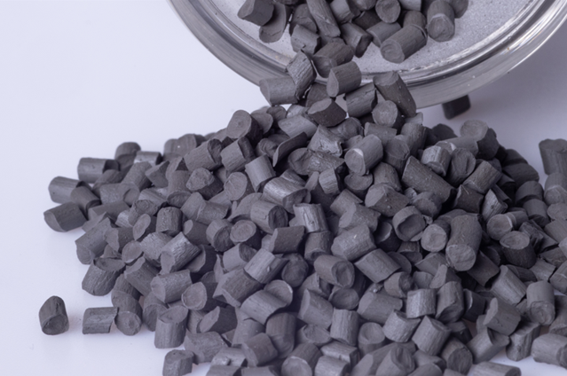
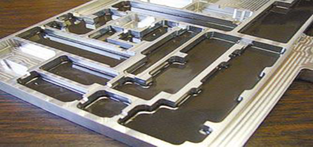
Most recently, many systems designers are discovering the need to make absorber material both structural and more “3D.” Increasingly in those cases, the selection of a thermoplastic absorber can lead to the creation of a cost-efficient, 3D-shaped design.
In the end, by approaching absorber selection holistically, no longer will you feel unready whenever discovering, “We have an EMI problem.”
Rick Johnson is a Business Development Manager of Laird, a DuPont business, based in Carlsbad, California, USA. He can be reached at [email protected]